|
Abstract: Preliminary
information. The placement of very high-performance PHEMT transistors and RFIC's, such as
the MGA-72543, in low-cost plastic packages gives rise to potential instability challenges
at high frequencies. This note provides a solution for stability at high frequencies.
(Addendum to Application Note RLM020199, "Designing with
the MGA-72543 RFIC Amplifier / Bypass Switch." )
The placement of very
high-performance PHEMT transistors and RFIC's, such as the MGA-72543, in low-cost plastic
packages gives rise to potential instability challenges at high frequencies.
The following graph shows the effect on stability
factor, K, of series inductance (shunt feedback) in the ground connection of the MGA-72543
RFIC. This graph is CAD-generated using the s-parameter data file for a bias condition of
20 mA. S-parameters are characterized in an extremely sterile test fixture in which both
ground pins of the MGA-72543 package are connected directly to RF ground. In this ideal
characterization environment the common lead inductance external to the package is
effectively zero. Note: Although the data sheet for the MGA-72543 lists s-parameters
up to 8 GHz, all of the *.s2p files for this device cover an actual measurement frequency
of 800 MHz to 12 GHz. This allows a very accurate analysis at high frequencies.
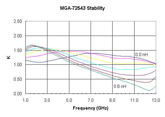
Figure 1. Stability
factor vs. Frequency vs. Ground Inductance.
The graph in Figure 1 shows the effect of common
lead inductance with values from 0 to 0.6 nH in 0.1 nH increments. As can be seen, an
inductance of only 0.2 nH is sufficient to cause concern for potential instability at
frequencies above 8 GHz. This analysis was performed with 25 �C data. At low operating
temperatures, device gain increases and the potential for instability is exacerbated.
It should be noted that the device's two ground
pins share the common lead inductance in a physical circuit. For simulation with a linear
CAD program, this means the common lead inductance is actually the parallel equivalent of
the inductance in both ground leads. For example, an inductance of 0.3 nH from each of the
device's ground pins to RF ground would be simulated in a CAD program by single inductor
of 0.15 nH.
This stability analysis illustrates the
importance of providing a low inductance path from each of the MGA-72543 ground pins to
the circuit's RF ground. In the case of this particular device, the ground pins are
generally not connected directly to RF ground but rather are capacitively bypassed to
allow a bias resistor to be placed between the ground pins and RF/DC ground. These bypass
capacitors contribute additional inductance to the device's ground path. This method of
source bypassing is similar to designing discrete FET circuits utilizing self-bias.
A lab test was conducted on an evaluation circuit
similar to that shown in Figure 13 of the MGA-72543 Application
Note. A sliding short was connected to the input of the amplifier and a spectrum
analyzer to the output. No instability was observed at room temperature for any position
of the sliding short. The MGA-72543 was then cooled by spraying with an aerosol coolant.
An oscillation was subsequently observed at approximately 9.9 GHz.
Since the CAD analysis and lab verification
indicates a potential instability at frequencies above 8 GHz, some stability
countermeasures are needed. Of the various techniques for increasing the K of a
potentially unstable circuit, one of the most practical is to use resistive loading.
Resistive loading at the input of the amplifier will not be considered in this case since
it would be detrimental to noise figure. Resistive loading can therefore be applied either
in series or in shunt at the output of the MGA-72543.
For bands of interest below approximately 3 GHz,
R-C or R-L combinations can be used to form a frequency selective resistive loading
circuit. This will stabilize the amplifier at high frequencies without affecting in-band
performance. For the MGA-72543, a parallel R-L in series with the output as shown in
Figure 2 provides a simple solution for potential instability with a negligible trade-off
in performance.

Figure 2. Parallel R-L
in Series With Output.
A CAD analysis of this solution with a common
lead inductance of 0.3 nH, indicates a 1.2 nH inductor in parallel with 50 - 100 ohms
provides a K > 1.5 from 1 GHz through 13 GHz. A plot of the resulting K vs. frequency
is shown in Figure 3. At frequencies in the X-band range, the reactance of the inductor is
fairly high, allowing the resistor to load the output of the amplifier. At frequencies of
2 GHz and below, the lower reactance of the inductor partially shorts the resistor to
minimize gain reduction. An additional benefit of the inductor at the output is an
improvement in output VSWR. The penalty in gain with the addition of the R-L circuit
is predicted to be 0.2 dB.
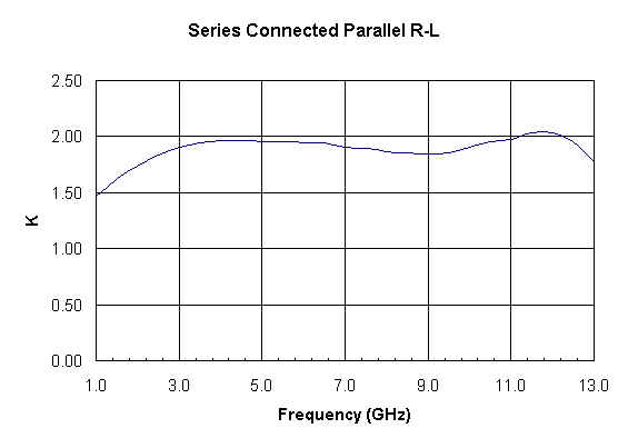
Figure 3. Stability
factor vs. Frequency with Parallel R-L in Output.
A modified evaluation circuit was used to test
the solution with a series connection of a parallel R-L at the output. In order to force
instability in the evaluation circuit, capacitor C4 in Figure 13 (of the Application Note)
was removed. This caused the circuit to oscillate at 10.5 GHz at room temperature. The
short-circuit jumper at the output of the evaluation circuit (labeled "SC" in
Figure 13) was replaced by a chip inductor of 1.8 nH in parallel with a resistor. A
resistor value of 82 ohms was found to suppress all oscillation.

Figure 4. Modified
Evaluation Circuit.
The gain of the original, unmodified evaluation
circuit was initially measured to be 13.73 dB at 2 GHz. Replacing the bypass capacitor at
Pin 1 of the stabilized circuit resulted in a 2 GHz gain of 13.5 dB. Consistent with CAD
analysis, the R-L at the output degraded gain by only approximately 0.2 dB.
Preliminary temperature tests (using aerosol
coolant) were conducted on the modified evaluation circuit with the following results:
"Forced
oscillation" circuit (ground pin bypass capacitor, C4, removed) -
no oscillation at room temperature; 10 GHz oscillation at low temperatures.
Re-installed C4
bypass capacitor immediately adjacent to the MGA-72543 ground pin (normal layout); no
oscillation observed from room temperature to extremely low temperatures.
Bypass capacitor C4 was re-positioned further from the
package ground pin to add a moderate amount of common lead inductance back into the
circuit. With C4 located adjacent C3, no oscillations were observed at low temperature.
This appears to be a very solid solution that can be
implemented quite easily on most circuit layouts.
Appendix A - MGA-72543 S-parameter
files
m72543v0.s2p (Bias current = 0
mA; Bypass switch mode)
m72543ib.s2p (Bias current = 5
mA; LNA mode)
m72543ic.s2p (Bias current = 10
mA; LNA mode)
m72543id.s2p (Bias current = 20
mA; LNA mode)
m72543ie.s2p (Bias current = 40
mA; Driver amplifier mode)
m72543if.s2p (Bias current = 60
mA; Driver amplifier mode)
|